Within the framework of a DFG priority programme, we are currently working on the development of an extremely broadband integrated photonic-electronic receiver on a silicon substrate.
Extreme broadband and reconfigurable integrated photonic electronic receiver on silicon substrate
Exceptionally high transmission capacities of optical communication systems can only be exploited by using electronic circuits in parallel, since the bandwidth of electronic circuits is fundamentally limited by the transit frequency of the available transistors. The developed electronic photonic integrated circuit (EPIC) enables extreme broadband and reconfigurable receivers on a single chip via photonic preprocessing followed by time interleaving electronic demultiplexing.
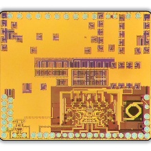
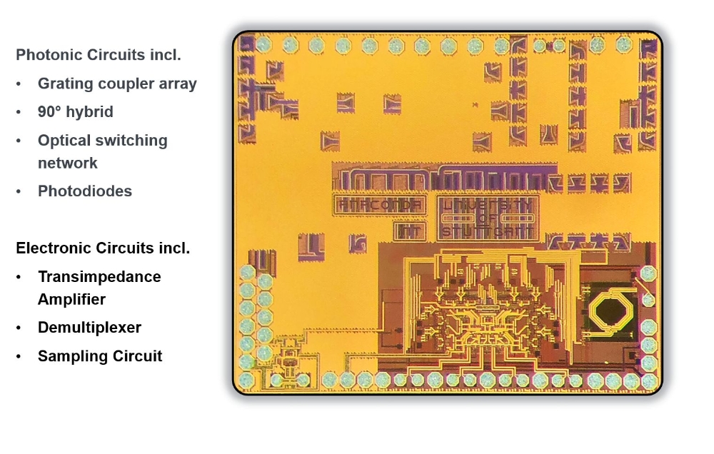
In common communication systems, the wide optical band with a spectrum in the THz range is subdivided into many small frequency bands (wavelength division multiplexing, WDM). The superimposed wavelength channels can be spectrally separated in the developed receiver by an integrated arrayed waveguide grating filter (AWG). Additional optical phase shifters in intermediate coupling structures of multimode interference couplers (MMIs) can select and route a specific wavelength channel. The conversion of the analog optical signal to a digital electronic signal is usually limited by the bandwidth of the analog-to-digital converters (ADC). To take full advantage of the large bandwidth of photodetectors and transimpedance amplifiers, an integrated 1:4 100 GBaud current demultiplexing circuit enables the parallel use of low-bandwidth ADCs. The monolithic approach chosen avoids any parasitic packaging inductance and capacitance that would reduce the bandwidth. Simulations have shown that the designed optoelectronic front end, consisting of photodiodes, transimpedance amplifier, and demultiplexer can sample 100 GBaud NRZ and 50 GBaud PAM4 optical signals, corresponding to a total data rate of 100 Gb/s. The developed optoelectronic circuits could potentially be used in future transceivers in data centers to realize a monolithic, broadband and flexible receiver.
Publications
2023
- R. Elster, N. Hoppe, M. Wittlinger, C. Schweikert, W. Vogel, M. Berroth, and G. Rademacher, “Versatile Optical Frequency Comb Generation: Modelling Silicon-Organic Hybrid Phase Shifters,” in Workshop: Ultrafast Signal Processing by Combined Photonic-Electronic Integrated Systems, 2023.
- J. Finkbeiner, P. Thomas, C. Schweikert, M. Grözing, M. Berroth, and G. Rademacher, “Monolithically Integrated Optoelectronic Receiver Front-End,” in Optica Advanced Photonics Congress: Workshop on Ultrafast Signal Processing by Combined Photonic-Electronic Integrated Systems, Busan, Republic of South Korea, 2023.
Additional Information
- DFG project
Extreme broadband integrated photonic electronic receiver on silicon substrate - DFG-SPP 2111
Integrated electronic-photonic systems for ultra-wideband signal processing
Contact
Jakob Finkbeiner
M. Sc.Research staff member

Wolfgang Vogel
Dr.-Ing.Senior Lecturer / Vice Director