For generations and analyzation of fast signals, the INT has numerous signal generators, oscilloscopes and network analyzers with a bandwidth of up to 67 GHz. The INT uses a wide range of devices from well-known manufacturers, such as Agilent, Anritsu, Keysight, Rohde & Schwarz, Teledyne LeCroy, Tektronix.

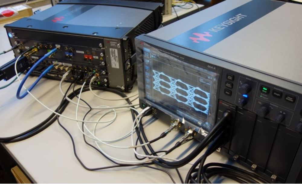
For the measurement of ultra-wideband electrical and optical signals, the "CrossLink" measurement system is available at INT and ILH.
For measurements in the time domain, the CrossLink system consists of an arbitrary waveform generator and a subsampling oscilloscope. Four differential signals can be generated with up to 65 GHz analog bandwidth at 128 GSa/s and detected with 122 GHz analog bandwidth.
The CrossLink system is funded by the German Science Foundation (DFG) in the frame of the major instrumentation initiative “Messsysteme für ultrahohe Datenraten für Kommunikationstechniken der Zukunft”.
For configuration of integrated circuits single-board computers (e.g., Raspberry Pi) or simple FPGAs (e.g., Xilinx Spartan 3) are commonly used.
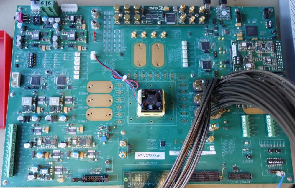
As an alternative to traditional metrology devices, FPGA development boards (eg, Xilinx Virtex-7, Virtex-6, and Virtex-4) are available with high-speed serial interfaces up to 28 Gbps per channel for both transmit and receive of data can be used. These channels can be grouped into multiple parallel interfaces.
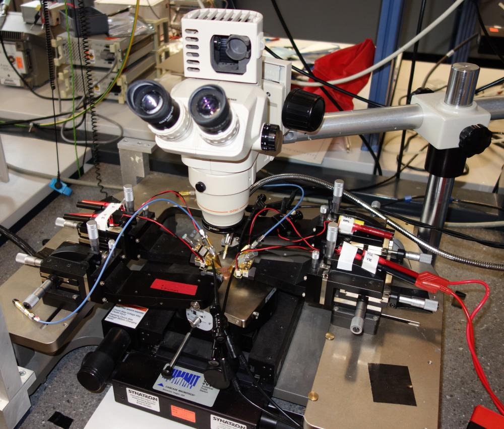
Instead of the packaging on printed circuit boards, integrated circuits with only a few connection pads can be connected directly to the measurement environment by means of a wafer prober. The contacting of the IC is done via measuring tips, which are aligned by means of micrometer manipulators under a microscope. The advantages are that the parasitic influences of the measuring tips and cables are generally much lower than those of the bonding wires and printed circuit board. Thus, this technique is suitable to characterize circuits with highest bandwidths. Hybrid setups are also possible. In this case, the power supply connections and low frequency configuration signals are supplied via a printed circuit board, while high-frequency signals are tapped via measuring tips.
Contact

Markus Grözing
Dr.-Ing.Group Leader Integrated Circuits