Packaging of integrated circuits requires highest precision. Therefore our laboratory is equipped with appropriate technology for the assembly of printed circuit boards with SMD components.
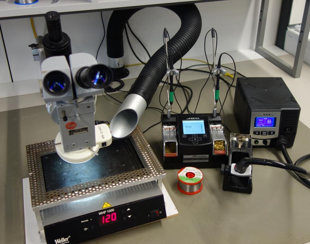
Soldering workstation
- Nano soldering station with microscope
- hot plate
- Hot air station
- Fume extraction unit
- Motor-driven soldering tip cleaning brushes
The assembly of printed circuit boards of the components is done manually. After soldering, the PCBs are cleaned in an ultrasonic bath with flux cleaner and distilled water to remove flux residues and other residues. The surface must be very clean for the subsequent bonding process.
The integrated circuits are usually glued for heat dissipation on a copper or brass plate and connected by means of bonding wires to a circuit board. The INT has corresponding bonding machines.
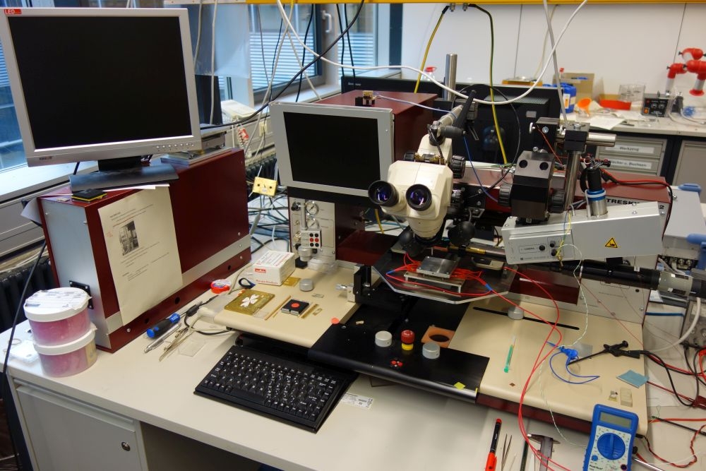
Bonding machines
The INT is equipped with
- Wedge bonder
- Ball bonder
- Die bonder
for gold and aluminum wire.
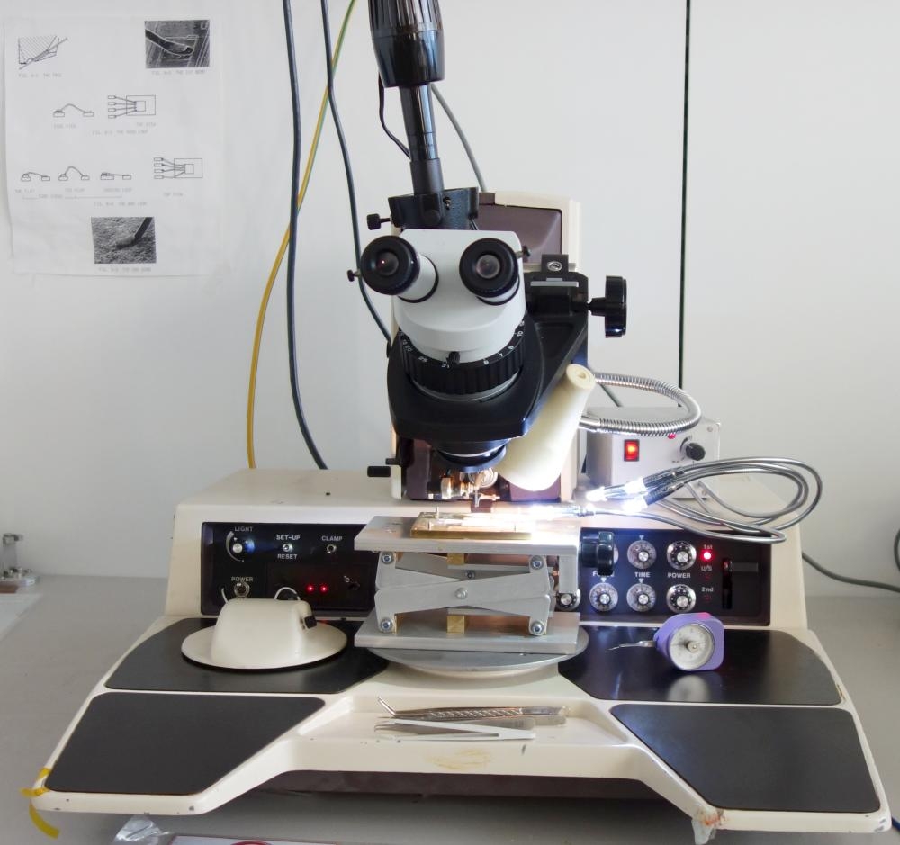
Our die bonder is a multifunctional bonding device. It can be used to place dies (sawn-out wafer pieces with integrated circuits) or packaged ICs on printed circuit boards. With the help of a camera with attached prism it is possible to view the component and the carrier at the same time, which allows an exact positioning of the components.
PCBs with packaged ICs can finally be soldered in an oven, with hot air or on a hot plate.
Dies with a small number of pads, which have previously been gold-bumped on our ball bonder, can be electrically bonded to a suitable substrate by means of thermocompression (so-called flip-chip bonding). For this purpose, a heated tool and a hot plate support the bonding process.
Further applications of the die bonder are the micrometer-accurate measurement of dies or the bonding of dies to printed circuit boards or in a cavity. The dies are then contacted conventionally by means of a wedge bonder.
Packaging examples
Example of a complex packaged integrated circuit. The IC is glued on a PCB and connected to the gold-plated board surface by gold bonding wires.
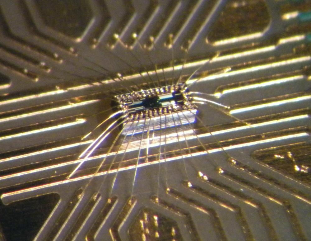
Example of a complete module with an integrated circuit. The IC is glued on a brass plate and connected to the gold-plated board surface by gold bonding wires.

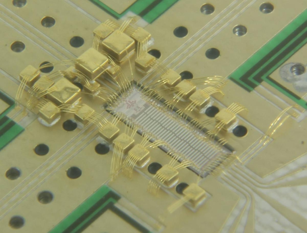
Close-up view of the packaged integrated circuit. The chip is sunk in a cavity. As a result, shorter lengths of bonding wires can be achieved. Bonding capacitances are placed close to the chip, which should compensate for voltage fluctuations.
Contact

Thomas Veigel
Dr.-Ing.Research staff member