The on-going growth of global data traffic drives optical data transmission systems beyond 1 Tbit/s per wavelength. Digital-to-analog converters (DACs) in transmitter front-ends are critical parts for the realization of such systems requiring sampling rates in the range of 100 GS/s and beyond. For monolithic integration with digital signal processors, CMOS DACs are essential.
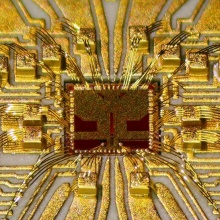
In this project, a full CMOS integration of two 8-bit sub-DACs and an active analog multiplexer (AMUX) on a single chip is realized in 28-nm FD-SOI CMOS for 100 GS/s and beyond for the first time. An additional on-chip 256-kB SRAM completes the system to a universal, single-chip arbitrary waveform generator (AWG). It comprises more than 14 million transistors. Generally, an AMUX is able to shift the limits of DACs in well-established CMOS technologies toward higher frequencies independent of technology advances and therefore, it opens a second, conceptual path for achieving higher sampling rates. The AWG is developed for optical communication experiments as well as for application in experimental setups requiring an ultra-fast AWG.
Broadband pulse-amplitude modulated (PAM) signals up to Nyquist frequency are demonstrated up to 108 GS/s (PAM-2) with data rates up to 240 Gbit/s (80 GS/s, PAM-8). At, 100 GS/s, PAM-4 signals are shown. Moreover, the DAC system can be used for oversampling applications and pulse shaping for sampling rates up to 118 GS/s at lower symbol rates.
Publications
2024
- D. Widmann, T. Tannert, X.-Q. Du, T. Veigel, M. Grözing, and M. Berroth, “A Time-Interleaved Digital-to-Analog Converter up to 118 GS/s With Integrated Analog Multiplexer in 28-nm FD-SOI CMOS Technology,” IEEE Journal of Solid State Circuits, vol. 59, pp. 908–922, 2024.
2023
- D. Widmann, M. Grözing, and M. Berroth, “Digital Time-Domain Predistortion of Linear Periodically Time-Varying Effects and Its Application to a 100-GS/s Time-Interleaved CMOS DAC,” IEEE Transactions on Circuits and Systems I: Regular Papers, vol. 70, pp. 5098–5109, 2023.
- D. Widmann, T. Tannert, M. Grözing, and M. Berroth, “Analog Multiplexer for Performance Enhancement of Digital-to-Analog Converters and Experimental 2-to-1 Time Interleaving in 28-nm FD-SOI CMOS,” IEEE Solid-State Circuits Letters, vol. 6, pp. 277–280, 2023.
2022
- D. Widmann, R. Nägele, M. Grözing, and M. Berroth, “Mixed-Signal Integrated Circuit for Direct Raised-Cosine Filter Waveform Synthesis of Digital Signals Up to 24 GS/s in 22 nm FD-SOI CMOS Technology,” in IEEE International Symposium on Circuits and Systems (ISCAS), 2022, p. paper ID 1248.
- D. Widmann, T. Tannert, X.-Q. Du, M. Grözing, and M. Berroth, “Multi-Phase Clock Path Circuit up to 57 GHz Including 5 bit Programmable Phase Interpolators for Time-Interleaved Broadband Data Converters in a 28 nm FD-SOI CMOS Technology,” in European Microwave Integrated Circuits Conference (EuMIC), 2022, pp. 177–180.
2018
- D. Widmann, M. Gözing, and M. Berroth, “High-Speed Serializer for a 64 GS s-1 Digital-to-Analog Converter in a 28 nm Fully-Depleted Silicon-on-Insulator CMOS Technology,” Advances in Radio Science, vol. 16, pp. 99–108, 2018.
2017
- T. Veigel, S. Brandl, and M. Grözing, “Speicher mit 1 Tbit/s Lesedurchsatz für einen sehr schnellen Arbiträrsignalgenerator in einer 28 nm FDSOI-CMOS-Technologie,” in Kleinheubacher Tagung, U.R.S.I. Landesausschuss in der Bundesrepublik Deutschland e.V, Miltenberg, Germany, 2017, pp. KH2017–Di.
- D. Widmann, M. Grözing, and M. Berroth, “A differential 19 channel 64 Gbit/s 16:1 multiplexer including a clock network in a 28 nm CMOS Fully-Depleted Silicon-on-Insulator technology,” in Kleinheubacher Tagung, U.R.S.I. Landesausschuss in der Bundesrepublik Deutschland e.V, Miltenberg, Germany, 2017, pp. KH2017–Di.
Additional Information
- DFG project
A high-speed power-efficient digital-to-analog converter in FDSOI CMOS for ultra-high bandwidth data transmission
Contact

Markus Grözing
Dr.-Ing.Group Leader Integrated Circuits


