The Institute of Electrical and Optical Communications Engineering has developed a digital-to-analog converter with a conversion rate of 100 GS/s and 8 bit nominal resolution in a 28 nm low power CMOS technology. One possible application is in the field of coherent optical transmission systems.
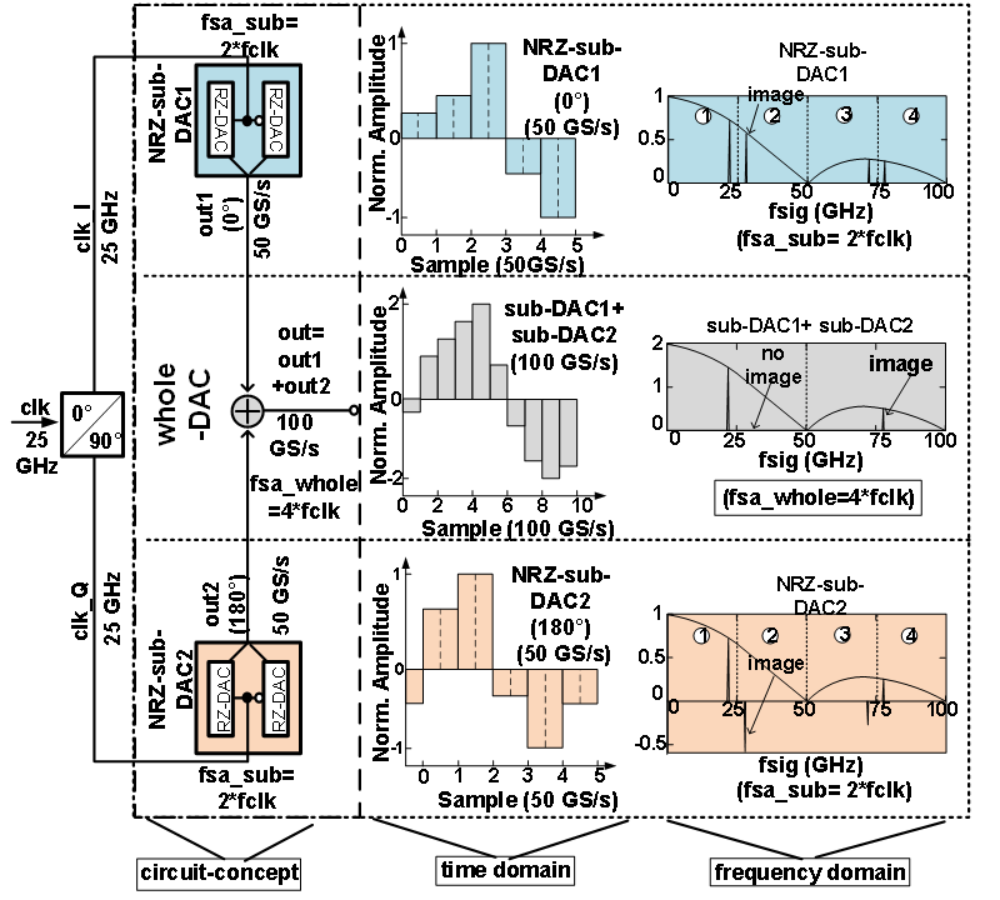
The following figure shows a block diagram of the DAC. The DAC prototype converts 1-k symbols stored in the 1-kbyte on-chip memory cyclically.

The DAC is set up of two time-interleaved 50 GS/s NRZ-sub-DACs. Each NRZ-sub-DAC is again set up of two time-interleaved 25 GS/s RZ-DACs. With this concept, the output signal images are located beyond 75 GHz for signal frequencies up to 25 GHz.
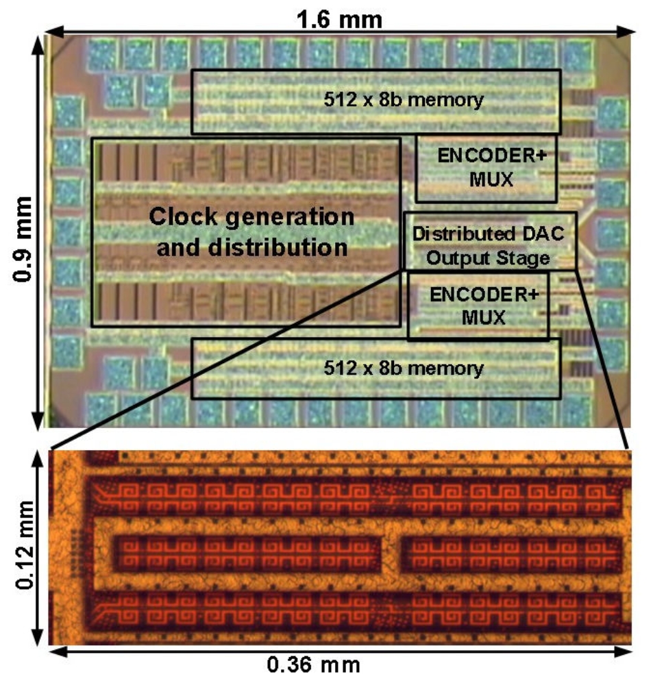
The following figure shows a chip micrograph. The DAC chip has an area of 1.44 mm² and consumes 2.5 W. The distributed DAC output current summation network is implemented as an artificial transmission line to enhance the output bandwidth.
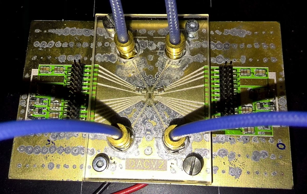
The DAC chip was measured on both on-wafer and on an RF-PCB.
The effective number of bits (ENOB) and spurious free dynamic range (SFDR) ranges from 5.3 bit and 41 dB to 3.2 bit and 27 dB from dc up to 24.9 GHz at 100 GS/s, respectively. The 3-dB bandwidth exceeds 13 GHz at 100 GS/s. The output signal roll off versus signal frequency is relatively flat resulting in 8 dB loss at 25 GHz including probes and cables to the 65 GHz bandwidth subsampling scope serving as a receiver.

The following figure shows an on-wafer measurement result of one sub-DAC. The output frequency response enables open output PAM8 eyes at 40 Gbaud without and with 10% digital pre-emphasis, corresponding to an effective output data rate of 120 Gbit/s.
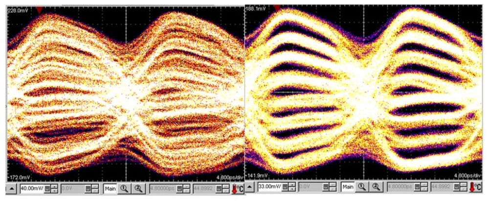
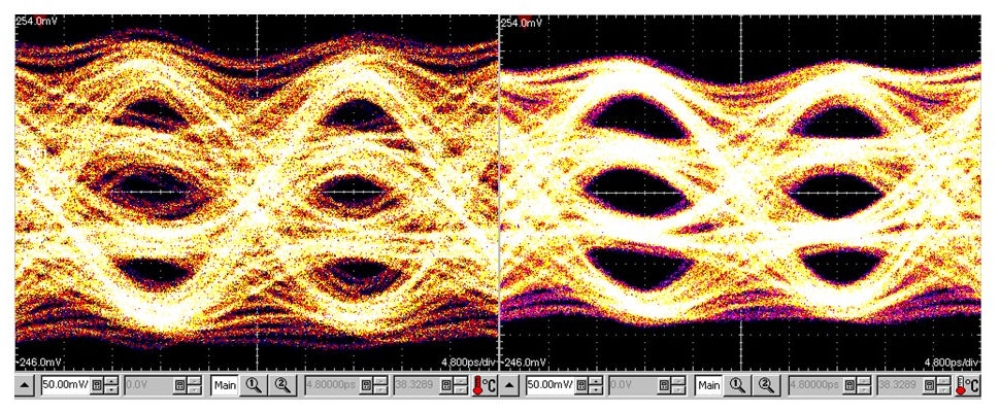
The following figure shows a measurement result of one sub-DAC on a PCB. It shows an open PAM4 eye at 50 GS/s without and woth pre-emphasis. The effective output data rate is 100 Gbit/s.
Publications
2016
- M. Grözing, H. Huang, X.-Q. Du, and M. Berroth, “Data converters for 100 Gbit/s communication links and beyond,” in Topical Meeting on Silicon Monolithic Integrated Circuits in RF Systems (SIRF). Digest of Papers, Austin, Texas, USA, 2016, p. pp. 104––106.
2015
- H. Huang, J. Heilmeyer, M. Grözing, M. Berroth, J. Leibrich, and W. Rosenkranz, “An 8-bit 100-GS/s Distributed DAC in 28-nm CMOS for Optical Communications,” IEEE Transactions on Microwave Theory and Techniques, vol. 63, pp. 1211–1218, 2015.
2014
- H. Huang, J. Heilmeyer, M. Grözing, and M. Berroth, “An 8-bit 100-GS/s distributed DAC in 28-nm CMOS,” in IEEE Radio Frequency Integrated Circuits Symposium (RFIC), Tampa, FL, USA, 2014, pp. 65–68.
Weiterführende Informationen
- 100 Milliarden Wandlungen pro Sekunde
Pressemitteilung der Universität Stuttgart (2. Juni 2014, Nr. 030)
Contact

Markus Grözing
Dr.-Ing.Group Leader Integrated Circuits