High-speed optical communication systems demand increasingly faster data conversion and signal processing. To address the bandwidth limitations of conventional digital-to-analog converters (DACs) in CMOS, time-interleaved architectures are widely adopted, where multiple DAC outputs are combined to generate a single ultra-high-speed analog signal.
This approach conserves the possibility for digital signal processing and signal generation in CMOS while enabling bandwidths far beyond single CMOS-DACs. The combining operation is performed by an analog multiplexer (AMUX), which must provide extremely precise, low-jitter, and high-speed switching. The application for AMUX-chips implemented in bipolar technology is broad reaching from ultra-broadband outputs of arbitrary waveform generators to high-speed communication links.
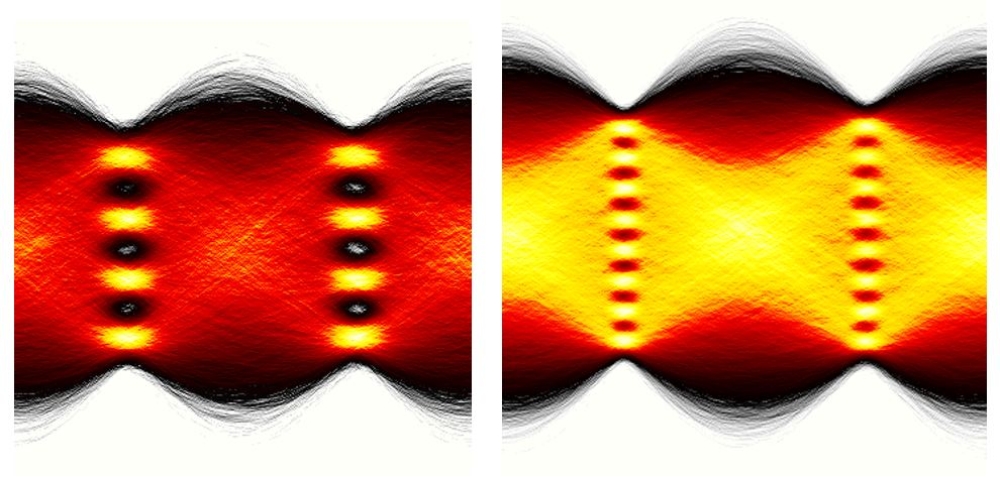
INT has developed a 2:1 analog multiplexer using IHP’s SG13G3 SiGe BiCMOS process, which is among the highest-speed semiconductor technologies reaching transit frequencies fT of 470 GHz and fmax of 650 GHz. The fabricated AMUX demonstrates a signal path with a bandwidth exceeding 110 GHz. The measured eye diagrams, including pre-EQ for PAM-4 at 150 GBd, and PAM-8 at 120 GBd are shown in Figure 1. Using the AMUX chip in a complete optical transmission setup, single-channel data rates of 467 Gbit/s have been shown. Further details and results can be found in the previous project ELAMUR (see link below).
The current project “OPTIMUX” strives to further push the limits of optical data transmission using analog multiplexing as well as space division multiplexing in glass fibers. The new AMUX generation is set to achieve a symbol rate of 300 GBd with an internal clk doubler, and a differential output swing of 2 V, enabling the AMUX to directly drive an electro-optical modulator (i.e. Mach Zehnder Modulator) without needing additional amplification.
The overall system architecture consists, in order, of a clock doubler, a cascade of clock amplifiers, the AMUX core, and an output amplifier, as shown in Figure 2.

The clock doubler must generate output frequencies in the range of 100–200 GHz with low duty cycle error, which are then routed through the clock path to drive the 2:1 AMUX core. It enables high-speed operation without requiring a 150 GHz signal source. In the clock path, a cascade of amplifiers is used to generate the signal strength to drive the current switches in the core. The AMUX core uses a Gilbert-cell-like structure to switch between the two input signals, yielding a time-interleaved signal of twice the symbol rate. Finally, a broadband linear output amplifier is employed to achieve the large differential voltage swing of 2 Vpp at a 50 Ohm matched output impedance.
Publications
2025
- M. Grözing, S. Özbek, J. Großholtfurth, S. Wazynski, T. Vollmer, S. Michel, and G. Rademacher, “Design of 200 GBd 22-nm CMOS-based and 300 GBd SiGe-HBT-based Analog Multiplexers,” in IEEE Photonics Society Summer Topicals Meeting Series (SUM), 2025, p. WB3.
- Q. Hu, M. Grözing, T. Tannert, R. Borkowski, F. Buchali, P. Iannone, G. Raybon, X. Chen, G. Rademacher, and R. Ryf, “High-Performance SiGe Analog Multiplexer Enabling 176 GBd PAM-8 Transmission,” Journal of Lightwave Technology, vol. 43, pp. 1881–1892, 2025.
2022
- J. Schostak, T. Tannert, C. Schmidt, H. Rucker, V. Jungnickel, M. Grözing, M. Berroth, and R. Freund, “150 GBd PAM-4 Electrical Signal Generation using SiGe-Based Analog Multiplexer IC,” in European Microwave Integrated Circuits Conference (EuMIC) 2022, 2022, pp. EuMIC13–3.
Additional Information
- Project page of the project sponsor [german]
Optimale Multiplexstrategien für die faseroptische Datenübertragung mit räumlichem Multiplex - Project page of the previous project ELAMUR
Broadband Analog Interleavers in BiCMOS
Contact

Fatemeh Ansari
M. Sc.Research staff member

Sefa Özbek
M. Sc.Research staff member

Tim Vollmer
M. Sc.Research staff member